

For decades, the semiconductor industry has relied on Moore’s Law which focuses on shrinking transistors to pack more computing power into smaller chips while improving efficiency. However, as the industry pushes towards 3nm and below, chipmakers are increasingly facing physical limitations, rising complexity and higher manufacturing costs.
At the same time, Huawei has been forced to explore alternative approaches due to ongoing US sanctions which cut the company off from advanced Western chipmaking technologies and access to leading foundries such as TSMC.
Despite these limitations, Huawei now appears to believe it has found a potential breakthrough to narrow the gap through a radically different chip architecture approach.
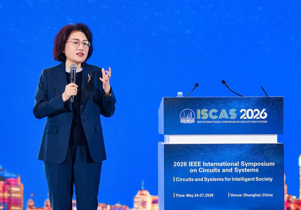
Huawei has recently introduced its “Tau (τ) Scaling Law” alongside a new chip architecture called “LogicFolding” during the IEEE International Symposium on Circuits and Systems (ISCAS) 2026 in Shanghai. Instead of focusing on shrinking transistors, Huawei is shifting its focus towards shortening the “time constant” inside chips to improve overall computing performance and efficiency.
Essentially, Huawei wants chips to process and move data more efficiently by reducing signal delays and shortening communication paths, instead of depending solely on increasingly expensive lithography advancements. As a result, Huawei says it can extract more performance from existing manufacturing technologies.
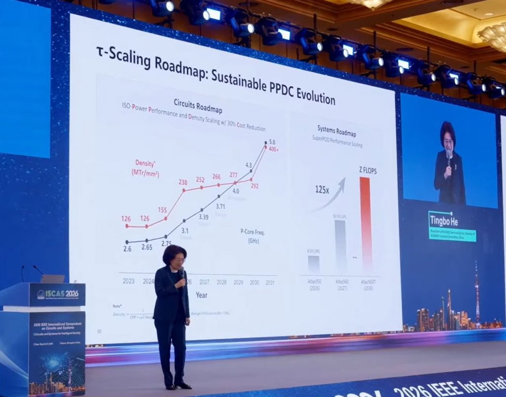
According to Huawei, this architectural approach could eventually achieve “1.4nm equivalent” performance by 2031. However, this does not mean Huawei is manufacturing chips on an actual 1.4nm process node. Instead, the company claims it can deliver similar transistor density and performance characteristics while still using more mature manufacturing processes such as 5nm or 7nm-class technologies.
This is seen as a potential game changer for Huawei as it currently faces heavy US sanctions which restrict access to advanced semiconductor manufacturing technologies, especially EUV lithography machines used by leading chipmakers such as Samsung and TSMC.
According to Huawei, its LogicFolding design offers multi-level co-optimisation that covers semiconductor devices, circuits, chips and systems.
At the device level, Huawei says it optimises the resistance and parasitic capacitance of transistors and interconnects to minimise the device-level time constant τ at the physical layer.
At the circuit level, the LogicFolding architecture breaks traditional circuit layout boundaries by significantly shortening critical-path wiring. Huawei says this reduces resistive and capacitive load during signal propagation while boosting transistor density and circuit performance.
At the chip level, Huawei says it uses a full-stack coordinated design involving software, architecture and silicon to achieve workload-driven control over instruction and data flows, improving parallelism and efficiency.
Finally, at the system level, Huawei says its UnifiedBus interconnect protocol enables unified memory addressing and native memory semantics to reduce communication latency across computing systems.
Huawei also claims it has already designed and mass-produced 381 chips over the past six years based on concepts related to Tau Scaling.
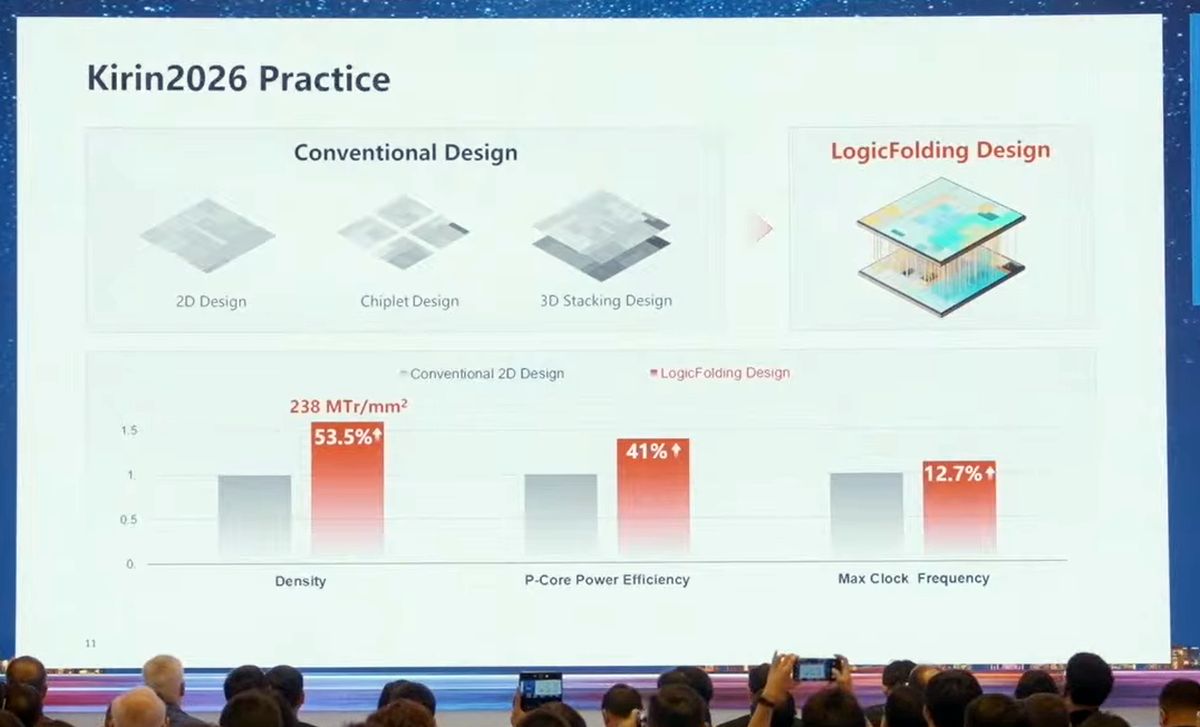
Their upcoming Kirin chip for the next Huawei mate series is expected to be their first commercial product with the LogicFolding architecture. It is said to be released sometime in the third quarter of this year with a transistor transistor density of 238 MTr/mm2 and clock speed of 3.1GHz.
Huawei claims its new architecture boast a 53.5% increase in transistor density (reaching 238 MTr/mm²), a 41% increase in performance-core power efficiency, and a 12.7% boost in maximum clock frequency (up to 3.1GHz) compared to conventional SoC design.
By 2031, Huawei targets a density of over 400+ MTr/mm² and clock speeds of 5.00GHz.
At the moment, Huawei has yet to officially reveal detailed benchmark figures for its products based on the new architecture.